Skip to content

Recent Posts

  • What to Look for in Shade Net Suppliers: A Comprehensive Guide
  • Corteiz cargos | crtz Official Store
  • The Role of Community Building in Scaling a Business
  • AI Receptionists vs. Traditional Staff: Which Saves More for Small Businesses?
  • Why Hire a React Native App Development Company for MVP Development

Most Used Categories

  • Other (1,446)
  • Lifestyle (658)
  • Watches (533)
  • Fashion (442)
  • Travel (193)
  • Sports (60)
  • Reviews (53)
Skip to content
Mycopywatches

Subscribe
  • Watches
  • Fashion
  • Lifestyle
  • Sports
  • Other
  • Reviews
  • Travel
  • Home
  • Other
  • Take our tips to correct these commercial painting mistakes
painting services

Take our tips to correct these commercial painting mistakes

admin1October 1, 2025October 1, 2025

Painting is a process that requires patience and attention to detail, and when we talk about commercial painting, it is a much bigger project than residential painting and requires utmost precision and perfection.

Well, the information below resembles all that you need to know about commercial painting mistakes and how to avoid them.

Major Factors Of Commercial Painting

Project Size

Commercial painting gigs are like tackling huge canvases like warehouses or sprawling retail spaces. They involve meticulous planning, specialized paints, and linger timelines to ensure durability and a polished finish. On the flip side, residential painting is more like working on a cozy portrait like a house or an apartment. It is quicker, with a focus on personal preferences and getting that homely feel just right. Both need skilled hands and attention to detail, just on different scales and vibes.

Quality Of Material Used

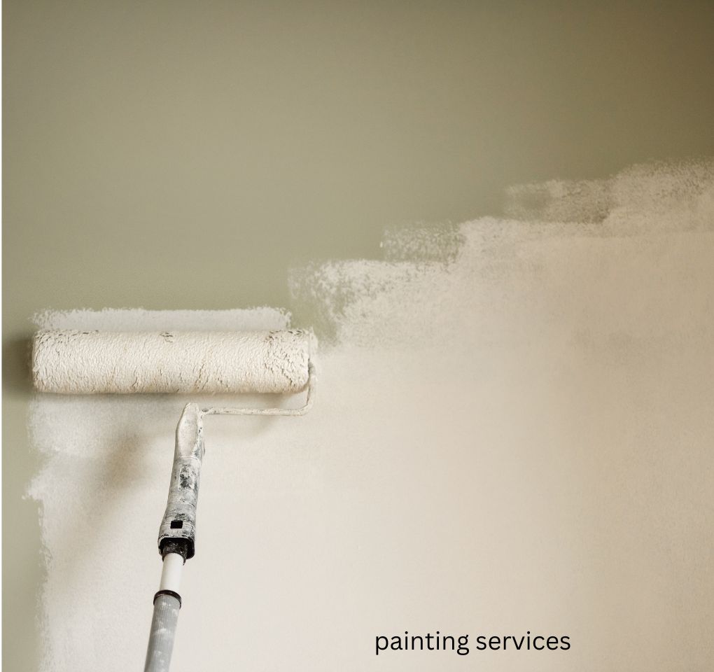
Material plays a big role in how the results show up, hence spending money on the right materials is quite essential in both commercial and residential painting work. Another thing to add is that in commercial work, there are specific equipment that are used so as to cover larger surfaces. Hence, the product quality of those materials should also be good. Also visit painting services in Dubai.

Painter Expertise

Commercial painters can handle everything from making sure bricks are waterproofed to fixing up concrete ceilings. Plus, they give metal doors a fresh coat to keep them looking sharp. Meanwhile, residential painters focus on making homes look amazing inside and out. They are all about painting walls, cabinets, and even hanging wallpaper to suit your style.

Common Commercial Painting Mistakes

Improper Planning

If you are gearing up for a big commercial painting job, but the planning gets a bit awry, then not only is the schedule all over the place but costs get creeping up too. Also, safety might be taking a hit if the concerned people have not thought about that properly. It is like trying a build a house without a blueprint because things just won’t hold up right.

Inexperienced Workers

When you have inexperienced folks on a commercial painting job, it can really throw a wrench into things. They might struggle to keep the paint smooth and even, leaving behind patches or streaks that just do not look pro. Plus, they often take more time to get the job done, which can mess with deadlines and tick off clients who are expecting things to move along smoothly.

Another factor is safety, as they might not be as familiar with how to handle themselves on scaffolding or around chemicals, which can be risky. And let us not forget about the materials as they can end up wasting paint or making mix-ups that cost the company. 

Using The Wrong Tool And Paint Products

This can definitely cause a lot of headaches as the job won’t look as good as it should be. You can imagine stuff like streaky finishes or uneven coverage, which does not exactly impress clients. Plus, using the wrong type of paint can lead to issues like peeling or fading sooner than expected, meaning more work down the line and higher costs.

On top of that, using inappropriate tools can slow things down, costing more labor and possibly delaying the whole project. Safety-wise, using tools incorrectly can be risky for everyone involved, and trying to cut costs with cheaper tools or paints might end up costing more in the long run if you have to redo things.

How Can You Avoid Common Commercial Painting Mistakes?

Do Proper Planning

Because the process is time-consuming and a lot of money is also involved, it is advised that a good plan should be made that covers all the necessary things from blueprints, complete map ideas, and the leaves as well. This way, sophisticated work shall begin and you will be prepared for any sudden issues that may arise while the painting goes on.

Make Sure Workers Work Safely

It is important to ensure the safety of workers in commercial painting jobs because these jobs often involve working at heights, using heavy equipment, and handling chemicals that can be dangerous if not used correctly. It is not just about following rules, it is about caring for the people doing the work.

Hire Professionals

When you hire genuine people who have some work experience in commercial painting, your stress eventually lowers because not only do you get good results but you can also discuss any alterations that need to happen. Since professionals have prior experience, they might give you the necessary suggestions that may save you time and money.

Also, you do not have to worry about safety or unexpected mishaps as they have got it covered with their insurance and guarantees. It is all about getting that wow factor for your space without the headaches.

Paint Wisely

What if you paint your outdoor deck with interior paint? It is going to fade and peel faster than you would think. And speaking of those cheap paints, they might look okay at first but can chip or change color sooner than you would like. Therefore, always go for good-quality paint that matches your project because it will save you a lot of trouble in the long run.

Make An Estimate Of The Total Expenses

So, when you partner with a professional estimator, you get someone who really digs into every detail of your project. They figure out exactly what materials you will need, how much labor it will take, and when everything can realistically be finished. This kind of thorough planning helps steer clear of any surprises that might slow things down or drive up costs unexpectedly.

Bottom Line

We hope that all the information given here proves to be a boon for anyone involved in commercial painting. The solutions and major factors given here and some of the most common ones (faced by almost everyone) and we hope that our points on how to avoid mistakes help you in every way possible!

Post navigation

Previous: Does Working with a Quartz Kitchen Tops Supplier Save Time?
Next: Roar into the Wild: Gir National Park Tour Packages for Nature Lovers and Big Cat Seekers

Related Posts

Shade Net Suppliers In UAE

What to Look for in Shade Net Suppliers: A Comprehensive Guide

October 1, 2025October 1, 2025 admin1

The Role of Community Building in Scaling a Business

October 1, 2025October 1, 2025 admin1
The semiconductor market is at a point of complex design growth that has never been experienced in history. As the transistors continue to reduce to the nanometer scale, more and more functions are being anticipated out of the modern chips. The modern System-on-Chip (SoC) designs also incorporate processors, memory, wireless connectivity, and security functions, and even AI accelerators, all in one package. This is a dynamite need to integrate, which poses unheard-of problems to engineers and semiconductor technology vendors. Electronic Design Automation (EDA), the collection of computer programs permitting chip designers to design, model, debug, and produce semiconductor gadgets, is the center of this change. However, conventional EDA tools are unable to bear the burden of the complexity of modern designs. To deal with these challenges, AI-based EDA is becoming a game changer as it enables companies to quickly develop products and also balance power, performance, and area (PPA) trade-offs more effectively than before. In the case of T2M-SEMI, which is the largest independent semiconductor technology provider in the world, AI-based solutions are not a choice anymore but a must. Having the knowledge in semiconductor IP cores, advanced SoC architectures, and disruptive technology, T2M-SEMI is on the leading edge of this change. The Growing Pressure on Semiconductor Design Increasing Complexity of SoC Architectures SoCs have become much more complex platforms as compared to relatively simple ones. An example of a modern smartphone chip can hold billions of transistors, a variety of CPUs and GPUs, AI accelerators, radio frequency systems, and sophisticated security measures. This integration requires not only impeccable functionality but also low power consumption, reduced die size, and shorter time-to-market. The conventional EDA processes find it difficult to handle such large complexity. Checks take more time, design bugs become more expensive, and the number of design cycles increases exponentially. The dilemma encountered by semiconductor firms is that the customers need the innovation to be very fast, whereas the tools needed to verify and simulate them tend to make the process slow. The Challenge of Scaling Beyond Moore’s Law The long-standing principle of Moore’s Law, which forecasted the doubling of the count of transistors every 2 years, has decelerated more rapidly. Rather, new performance gains are solely supported by architectural innovation, improved packaging, and heterogeneous integration. Such trends bring about a new dimension of complexity that cannot be addressed using the traditional methods. But AI-based EDA applications are already showing the ability to automatically perform optimization steps that used to take months to hand-write. How AI is Reshaping EDA Automation of Time-Consuming Processes Among the short-term advantages of AI in EDA are the automation of design processes that are labor-intensive. Machine learning algorithms are able to process thousands of design options and propose the best floor plans, routing layouts, or power allocation plans. This automation saves on manual intervention and frees the engineers to think at a higher level of architectural innovation. Predictive Analytics for Faster Verification Depending on the semiconductor design, verification has always been one of the most resource-intensive steps. Predictive analytics with artificial intelligence (AI) capabilities will be able to detect possible design defects at the initial stage of design, minimizing expensive reiterations at the design stage. Through past design information, AI models are able to spot problems that are not evident during standard testing, resulting in more trustworthy chip designs. Enhancing PPA Optimization The eventual aim of semiconductor design is the balancing of performance, power, and area. Multi-variable optimization EDA tools based on AI are particularly effective to evaluate the trade-offs in an unlimited number of design dimensions. Rather than using trial and error techniques, engineers can use AI to arrive at the most efficient solution faster. T2M-SEMI: Leading the Way in AI-Enhanced Semiconductor Solutions A Global Independent Technology Provider T2M-SEMI is the biggest independent global provider of semiconductor technology and is therefore very critical in facilitating innovation in various industries. The company deals with the delivery of semiconductor IP cores, silicon-proven subsystems, KGD, software, and disruptive technologies used to deliver customers throughout the globe with technologies faster time-to-market. Incorporating AI-enhanced EDA into its portfolio, T2M-SEMI does not merely react to the difficulties in the industry but proactively determines the course of action. The capability to offer pre-verified, silicon-proven IP blocks enables companies to avoid lengthy development cycles, whereas AI-based EDA integration guarantees smooth compatibility to unique SoC needs. Enabling System-on-Chip Innovation Starting afresh is no longer an option to companies developing next-generation SoCs. Risk reduction (licensing of proven semiconductor IP cores by providers such as T2M-SEMI) and innovation speed up innovation. In combination with AI-driven design software, these cores can be designed even quicker, checked with increased reliability, and tailored to a variety of applications, including IoT and automotive, 5G, and AI accelerators. Industry Impact: From IoT to AI and Automotive IoT and Edge Devices In the Internet of Things, the chips will need to integrate a combination of low power consumption and dependable connectivity. The EDA technologies based on AI can facilitate the process of designing small, efficient chips that can address these high requirements. The portfolio of wireless and interface IP solutions of T2M-SEMI, supported with AI-optimized workflows, allows the manufacturers of IoT devices to introduce their devices quicker with no compromise in quality. Automotive Semiconductors The automotive systems require fault tolerance, safety requirements, and real-time performance. As the concept of autonomous driving grew, the complexity of automotive SoCs has increased exponentially. AI EDA is susceptible to automated verification processes, which minimize risk and result in the automotive-grade chip fulfilling functional safety constraints without undue delays. AI and Machine Learning Accelerators Ironically, even AI has to be operated with highly specialized chips in order to do so effectively. AI accelerator design is done in the context of parallelism, memory bandwidth, and thermal limits. In this case, AI-based EDA tools are particularly useful, as they can automatically search the design space to find the architectures that provide the best performance when running machine learning workloads. T2M-SEMI, through its broad set of IP cores and system-level solutions, helps customers to accelerate the market with AI accelerators. Overcoming Challenges in AI-Driven EDA Data Dependency The performance of AI models is determined by the data used to train them. The success and failure of designs have to be collected into large datasets in order to be as accurate as possible with the use of EDA tools. The providers of semiconductor technology should also invest in building solid data pipes and yet maintain data secrecy for their clients. Integration with Legacy Workflows Numerous firms make use of the well-established toolchains of EDA. The biggest challenge is to integrate AI capabilities without causing any disturbance to the current working processes. By integrating AI solutions into their established IP and SoC development models, providers such as T2M-SEMI facilitate this by reducing friction on the part of end-users. Trust and Transparency Engineers are used to clear-cut, deterministic work flows. The uncertainty involved by the AI can occasionally be a source of hesitation. To be able to widely adopt AI-driven decisions, it is crucial to be able to achieve transparency, explainability, and traceability. The Future of AI in Semiconductor Design Towards Fully Autonomous Design The dream of complete chip design autonomy, where AI-assisted EDA systems can accept specifications and produce optimized layouts automatically, is no longer science fiction. Although human expertise will never be less important, AI is already coming close to a place where it can do much of the design exploration and optimization automatically. Expanding Beyond Design to Manufacturing Design will not be the only part to stop AI. The AI algorithms are already employed in semiconductor manufacturing to predict defects in the yield process, to optimize the parameters of the process, and to desire closer quality control. This collaboration between the AI-assisted design and AI-assisted manufacturing will establish a smooth end-to-end semiconductor development pipeline. Redefining the Role of Technology Providers The emergence of AI-based EDA tools is a semiconductor design paradigm shift. AI is addressing the challenge of design complexity, speeding up the verification process, and making faster innovation possible, which is enabling semiconductor firms to keep up with the industry. The introduction of AI into EDA processes is both a challenge and an opportunity to semiconductor technology providers such as T2M-SEMI. T2M-SEMI is in the market with the right knowledge of semiconductor IP cores, disruptive SoC technologies, and a global network of partners, and it is in a position to spearheadthis transition. The era of unprecedented complexity and innovation in the industry is upon us, and AI-driven EDA is not a tool but the basis on which the next generation of semiconductors will be developed.

AI Receptionists vs. Traditional Staff: Which Saves More for Small Businesses?

October 1, 2025October 1, 2025 admin1

Leave a Reply Cancel reply

Your email address will not be published. Required fields are marked *

  • What to Look for in Shade Net Suppliers: A Comprehensive Guide
  • Corteiz cargos | crtz Official Store
  • The Role of Community Building in Scaling a Business
  • AI Receptionists vs. Traditional Staff: Which Saves More for Small Businesses?
  • Why Hire a React Native App Development Company for MVP Development
admin1 Avatar
Pinterest
Gravatar
Blogger
Reddit
Medium
Linktree
Issuu
Pixabay
Goodreads
Mixcloud
500px
Walkscore
Gitee
Sketchfab
Habr QnA
MagCloud
Solo.to
GiantBomb
StockTwits
Designspiration
Mbed
Biolinky
Canadian Geographic PhotoClub
Experiment
Dermandar
Copyright All Rights Reserved | Theme: BlockWP by Candid Themes.