Skip to content

Recent Posts

  • What to Look for in Shade Net Suppliers: A Comprehensive Guide
  • Corteiz cargos | crtz Official Store
  • The Role of Community Building in Scaling a Business
  • AI Receptionists vs. Traditional Staff: Which Saves More for Small Businesses?
  • Why Hire a React Native App Development Company for MVP Development

Most Used Categories

  • Other (1,446)
  • Lifestyle (658)
  • Watches (533)
  • Fashion (442)
  • Travel (193)
  • Sports (60)
  • Reviews (53)
Skip to content
Mycopywatches

Subscribe
  • Watches
  • Fashion
  • Lifestyle
  • Sports
  • Other
  • Reviews
  • Travel
  • Home
  • Other
  • How Long Do Hypertherm Consumables Last in Industrial Use?

How Long Do Hypertherm Consumables Last in Industrial Use?

admin1October 1, 2025October 1, 2025

In the world of plasma cutting, the quality of consumables is one of the most important factors that determine performance, accuracy, and cost-effectiveness. Many brands manufacture consumables, but one name that stands out across industries worldwide is Hypertherm. Professionals trust Hypertherm not only for their cutting systems but also for their consumables and parts.

So, what makes Hypertherm Consumables different from other brands? Why do professionals and industries prefer Hypertherm Consumable & Parts over cheaper alternatives? Let’s take a detailed look.

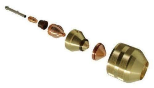
What Are Hypertherm Consumables?

Before we understand what makes them unique, let’s first define them. Hypertherm consumables are the replaceable components inside a plasma cutting torch that wear out with use. They are essential for generating and controlling the plasma arc that cuts through metal.

The main Hypertherm consumables include:

  • Electrode – Creates and maintains the plasma arc.
  • Nozzle – Shapes and directs the plasma jet for accuracy.
  • Swirl Ring – Controls gas flow and keeps the arc stable.
  • Shield – Protects both the nozzle and workpiece during cutting.
  • Retaining Cap – Holds all the consumables securely in place.

These Hypertherm Consumable & Parts work together to ensure clean, efficient, and reliable cutting.

What Makes Hypertherm Consumables Different?

There are several reasons why Hypertherm consumables stand apart from other brands:

1. Precision Engineering

Hypertherm consumables are designed with advanced engineering and strict quality standards. Every nozzle, electrode, and shield is manufactured to exact tolerances, ensuring consistent cutting results. Other brands often compromise on design accuracy, leading to unstable arcs and poor cut quality.

2. Longer Life with Advanced Technology

One of the biggest differences is the long life technology that Hypertherm uses in its consumables. For example, their LongLife electrodes are built with advanced cooling designs that increase lifespan and reduce wear. This means fewer replacements compared to generic consumables, saving both time and money.

3. Consistent Performance

While cheaper consumables may give good results initially, they often lose performance quickly. Hypertherm consumables are designed to maintain consistent cutting speed, arc stability, and edge quality throughout their usable life. This consistency is highly valued in professional workshops and industries.

4. Better Cutting Quality

Hypertherm consumables deliver cleaner, smoother cuts with minimal dross. This reduces the need for secondary operations such as grinding or finishing. Competing brands often produce cuts with rough edges or more slag, which increases rework time.

5. Torch Protection

Using poor-quality consumables can damage the plasma torch itself, leading to costly repairs or replacements. Hypertherm consumables are specifically designed to protect the torch, ensuring long-term machine life and fewer breakdowns.

6. Cost Savings in the Long Run

While Hypertherm consumables may appear more expensive upfront, they actually save money in the long term. Their durability, consistency, and reduced rework time make them more economical compared to cheaper brands that require frequent replacements.

7. Safety and Reliability

Every Hypertherm consumable undergoes strict quality testing to ensure safety. Generic or counterfeit consumables often fail these standards, increasing the risk of arc instability, overheating, or accidents. Professionals choose Hypertherm because reliability and safety are never compromised.

Comparing Hypertherm Consumables with Other Brands

Let’s compare Hypertherm consumables with generic or cheaper alternatives:

FeatureHypertherm ConsumablesOther Brands
Cut QualitySmooth, accurate, minimal drossRough edges, more rework needed
DurabilityLonger life due to advanced designWear out quickly
ConsistencyStable performance throughoutDeclining performance over time
Torch ProtectionProtects torch from damageMay damage torch
Cost-EffectivenessSaves money in long runFrequent replacements increase cost
SafetyStrictly tested for safetyMay fail under heavy use

This table clearly shows why Hypertherm Consumable & Parts are the smarter choice for professionals.

Why Professionals Trust Hypertherm

Professionals around the world choose Hypertherm because:

  • They get consistent, high-quality results every time.
  • They can rely on consumables that last longer.
  • Their cutting torches remain protected.
  • They save both time and money by reducing downtime and rework.
  • They know safety is never compromised.

These benefits explain why Hypertherm has built a strong reputation as the industry leader in plasma cutting technology.

Tips to Get the Best Out of Hypertherm Consumables

Even the best consumables require proper handling. Professionals follow these practices:

  1. Always use genuine Hypertherm Consumable & Parts.
  2. Replace consumables before they are fully worn out.
  3. Match the consumables with the correct torch model and amperage.
  4. Keep the torch and consumables clean.
  5. Avoid mixing genuine and low-quality parts.

By following these tips, users can maximize the performance and lifespan of their consumables.

Conclusion

So, what makes Hypertherm Consumables different from other brands? The answer lies in their precision, durability, consistency, and safety. Unlike cheaper alternatives, Hypertherm Consumable & Parts provide clean cuts, longer torch life, and real cost savings in the long run.

Professionals around the world prefer Hypertherm because they know that in industries where quality and reliability matter, there is no substitute for genuine Hypertherm consumables. Choosing them is not just a purchase—it’s an investment in better performance, safety, and long-term success.

#HyperthermConsumableAndParts, #HyperthermConsumables, #MetalCuttingSolutions, #PlasmaCutting

Post navigation

Previous: Logo Greaseproof Paper A Complete Guide for Businesses
Next: Gautam Rice: The Premium Choice for Every Kitchen

Related Posts

Shade Net Suppliers In UAE

What to Look for in Shade Net Suppliers: A Comprehensive Guide

October 1, 2025October 1, 2025 admin1

The Role of Community Building in Scaling a Business

October 1, 2025October 1, 2025 admin1
The semiconductor market is at a point of complex design growth that has never been experienced in history. As the transistors continue to reduce to the nanometer scale, more and more functions are being anticipated out of the modern chips. The modern System-on-Chip (SoC) designs also incorporate processors, memory, wireless connectivity, and security functions, and even AI accelerators, all in one package. This is a dynamite need to integrate, which poses unheard-of problems to engineers and semiconductor technology vendors. Electronic Design Automation (EDA), the collection of computer programs permitting chip designers to design, model, debug, and produce semiconductor gadgets, is the center of this change. However, conventional EDA tools are unable to bear the burden of the complexity of modern designs. To deal with these challenges, AI-based EDA is becoming a game changer as it enables companies to quickly develop products and also balance power, performance, and area (PPA) trade-offs more effectively than before. In the case of T2M-SEMI, which is the largest independent semiconductor technology provider in the world, AI-based solutions are not a choice anymore but a must. Having the knowledge in semiconductor IP cores, advanced SoC architectures, and disruptive technology, T2M-SEMI is on the leading edge of this change. The Growing Pressure on Semiconductor Design Increasing Complexity of SoC Architectures SoCs have become much more complex platforms as compared to relatively simple ones. An example of a modern smartphone chip can hold billions of transistors, a variety of CPUs and GPUs, AI accelerators, radio frequency systems, and sophisticated security measures. This integration requires not only impeccable functionality but also low power consumption, reduced die size, and shorter time-to-market. The conventional EDA processes find it difficult to handle such large complexity. Checks take more time, design bugs become more expensive, and the number of design cycles increases exponentially. The dilemma encountered by semiconductor firms is that the customers need the innovation to be very fast, whereas the tools needed to verify and simulate them tend to make the process slow. The Challenge of Scaling Beyond Moore’s Law The long-standing principle of Moore’s Law, which forecasted the doubling of the count of transistors every 2 years, has decelerated more rapidly. Rather, new performance gains are solely supported by architectural innovation, improved packaging, and heterogeneous integration. Such trends bring about a new dimension of complexity that cannot be addressed using the traditional methods. But AI-based EDA applications are already showing the ability to automatically perform optimization steps that used to take months to hand-write. How AI is Reshaping EDA Automation of Time-Consuming Processes Among the short-term advantages of AI in EDA are the automation of design processes that are labor-intensive. Machine learning algorithms are able to process thousands of design options and propose the best floor plans, routing layouts, or power allocation plans. This automation saves on manual intervention and frees the engineers to think at a higher level of architectural innovation. Predictive Analytics for Faster Verification Depending on the semiconductor design, verification has always been one of the most resource-intensive steps. Predictive analytics with artificial intelligence (AI) capabilities will be able to detect possible design defects at the initial stage of design, minimizing expensive reiterations at the design stage. Through past design information, AI models are able to spot problems that are not evident during standard testing, resulting in more trustworthy chip designs. Enhancing PPA Optimization The eventual aim of semiconductor design is the balancing of performance, power, and area. Multi-variable optimization EDA tools based on AI are particularly effective to evaluate the trade-offs in an unlimited number of design dimensions. Rather than using trial and error techniques, engineers can use AI to arrive at the most efficient solution faster. T2M-SEMI: Leading the Way in AI-Enhanced Semiconductor Solutions A Global Independent Technology Provider T2M-SEMI is the biggest independent global provider of semiconductor technology and is therefore very critical in facilitating innovation in various industries. The company deals with the delivery of semiconductor IP cores, silicon-proven subsystems, KGD, software, and disruptive technologies used to deliver customers throughout the globe with technologies faster time-to-market. Incorporating AI-enhanced EDA into its portfolio, T2M-SEMI does not merely react to the difficulties in the industry but proactively determines the course of action. The capability to offer pre-verified, silicon-proven IP blocks enables companies to avoid lengthy development cycles, whereas AI-based EDA integration guarantees smooth compatibility to unique SoC needs. Enabling System-on-Chip Innovation Starting afresh is no longer an option to companies developing next-generation SoCs. Risk reduction (licensing of proven semiconductor IP cores by providers such as T2M-SEMI) and innovation speed up innovation. In combination with AI-driven design software, these cores can be designed even quicker, checked with increased reliability, and tailored to a variety of applications, including IoT and automotive, 5G, and AI accelerators. Industry Impact: From IoT to AI and Automotive IoT and Edge Devices In the Internet of Things, the chips will need to integrate a combination of low power consumption and dependable connectivity. The EDA technologies based on AI can facilitate the process of designing small, efficient chips that can address these high requirements. The portfolio of wireless and interface IP solutions of T2M-SEMI, supported with AI-optimized workflows, allows the manufacturers of IoT devices to introduce their devices quicker with no compromise in quality. Automotive Semiconductors The automotive systems require fault tolerance, safety requirements, and real-time performance. As the concept of autonomous driving grew, the complexity of automotive SoCs has increased exponentially. AI EDA is susceptible to automated verification processes, which minimize risk and result in the automotive-grade chip fulfilling functional safety constraints without undue delays. AI and Machine Learning Accelerators Ironically, even AI has to be operated with highly specialized chips in order to do so effectively. AI accelerator design is done in the context of parallelism, memory bandwidth, and thermal limits. In this case, AI-based EDA tools are particularly useful, as they can automatically search the design space to find the architectures that provide the best performance when running machine learning workloads. T2M-SEMI, through its broad set of IP cores and system-level solutions, helps customers to accelerate the market with AI accelerators. Overcoming Challenges in AI-Driven EDA Data Dependency The performance of AI models is determined by the data used to train them. The success and failure of designs have to be collected into large datasets in order to be as accurate as possible with the use of EDA tools. The providers of semiconductor technology should also invest in building solid data pipes and yet maintain data secrecy for their clients. Integration with Legacy Workflows Numerous firms make use of the well-established toolchains of EDA. The biggest challenge is to integrate AI capabilities without causing any disturbance to the current working processes. By integrating AI solutions into their established IP and SoC development models, providers such as T2M-SEMI facilitate this by reducing friction on the part of end-users. Trust and Transparency Engineers are used to clear-cut, deterministic work flows. The uncertainty involved by the AI can occasionally be a source of hesitation. To be able to widely adopt AI-driven decisions, it is crucial to be able to achieve transparency, explainability, and traceability. The Future of AI in Semiconductor Design Towards Fully Autonomous Design The dream of complete chip design autonomy, where AI-assisted EDA systems can accept specifications and produce optimized layouts automatically, is no longer science fiction. Although human expertise will never be less important, AI is already coming close to a place where it can do much of the design exploration and optimization automatically. Expanding Beyond Design to Manufacturing Design will not be the only part to stop AI. The AI algorithms are already employed in semiconductor manufacturing to predict defects in the yield process, to optimize the parameters of the process, and to desire closer quality control. This collaboration between the AI-assisted design and AI-assisted manufacturing will establish a smooth end-to-end semiconductor development pipeline. Redefining the Role of Technology Providers The emergence of AI-based EDA tools is a semiconductor design paradigm shift. AI is addressing the challenge of design complexity, speeding up the verification process, and making faster innovation possible, which is enabling semiconductor firms to keep up with the industry. The introduction of AI into EDA processes is both a challenge and an opportunity to semiconductor technology providers such as T2M-SEMI. T2M-SEMI is in the market with the right knowledge of semiconductor IP cores, disruptive SoC technologies, and a global network of partners, and it is in a position to spearheadthis transition. The era of unprecedented complexity and innovation in the industry is upon us, and AI-driven EDA is not a tool but the basis on which the next generation of semiconductors will be developed.

AI Receptionists vs. Traditional Staff: Which Saves More for Small Businesses?

October 1, 2025October 1, 2025 admin1

Leave a Reply Cancel reply

Your email address will not be published. Required fields are marked *

  • What to Look for in Shade Net Suppliers: A Comprehensive Guide
  • Corteiz cargos | crtz Official Store
  • The Role of Community Building in Scaling a Business
  • AI Receptionists vs. Traditional Staff: Which Saves More for Small Businesses?
  • Why Hire a React Native App Development Company for MVP Development
admin1 Avatar
Pinterest
Gravatar
Blogger
Reddit
Medium
Linktree
Issuu
Pixabay
Goodreads
Mixcloud
500px
Walkscore
Gitee
Sketchfab
Habr QnA
MagCloud
Solo.to
GiantBomb
StockTwits
Designspiration
Mbed
Biolinky
Canadian Geographic PhotoClub
Experiment
Dermandar
Copyright All Rights Reserved | Theme: BlockWP by Candid Themes.